Hitachi’s Holography Electron Microscope Attains Unprecedented Resolution
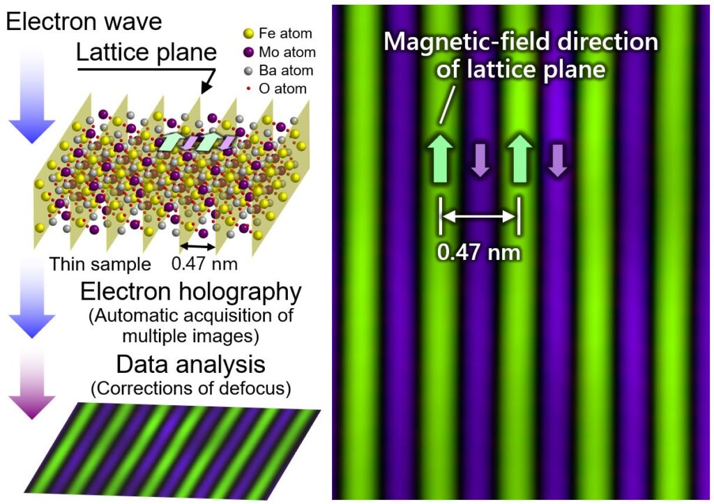
Image acquisition and defocusing correction techniques enable observations of atomic-scale magnetic fields at never-before-seen resolution
Electron holography microscopy is an advanced technique that can be used to visualize magnetic fields in materials at atomic resolution. In a recent study, researchers from Japan addressed some key limitations in this technique, achieving a groundbreaking resolution of 0.47 nm when imaging magnetic atomic lattices in a crystal. Their efforts could pave the way for scientific discoveries in materials science and notable sustainability improvements in electronics, energy generation, and other applied fields.
Tokyo, Japan—A research team from Japan, including scientists from Hitachi, Ltd. (TSE 6501, Hitachi), Kyushu University, RIKEN, and HREM Research Inc. (HREM), has achieved a major breakthrough in the observation of magnetic fields at unimaginably small scales. In collaboration with National Institute of Advanced Industrial Science and Technology (AIST) and the National Institute for Materials Science (NIMS), the team used Hitachi’s atomic-resolution holography electron microscope—with a newly developed image acquisition technology and defocus correction algorithms—to visualize the magnetic fields of individual atomic layers within a crystalline solid.
Many advances in electronic devices, catalysis, transportation, and energy generation have been made possible by the development and adoption of high-performance materials with tailored characteristics. Atom arrangement and electron behavior are among the most critical factors that dictate a crystalline material’s properties. Notably, the orientation and strength of magnetic fields right at the interface between different materials or atomic layers are particularly important, and often help explain many peculiar physical phenomena. Prior to this breakthrough, the maximum resolution at which the magnetic field of atomic layers could be observed was limited to around 0.67 nm, a record set by Hitachi using their cutting-edge holography electron microscope in 2017.
Now, thanks to a large collaborative project, researchers have managed to push this limit even further by addressing a few key limitations in Hitachi’s holography electron microscope. Their findings have been published in the journal Nature on July 03, 2024.
The researchers first developed a system to automate the control and tuning of the device during data acquisition, significantly speeding up the imaging process to a speed of 10,000 images over 8.5 hours. Then, by performing specific averaging operations with these images, they minimized noise to obtain much clearer images containing distinct electric field and magnetic field data.
The challenge addressed next was the correction for minute defocusing, which caused aberrations in the acquired images. “The idea of post-image-capture correction of aberrations we employed is exactly the same as that which had motivated Dr. Dennis Gabor to invent electron holography in 1948. In other words, the methodology was already theoretically established. Until now, however, there had been no technological implementations for such automated correction in off-axis electron holography,” explains Chief Researcher Toshiaki Tanigaki from Hitachi, Ltd. The technique implemented was able to correct for defocusing due to minor focus shifts by analyzing reconstructed electron waves. Thanks to this approach, the resulting images were free of residual aberrations, making the positions and phases of atoms easily discernible with magnetic field.
Leveraging these two innovations, the team performed electron holography measurements on samples of Ba2FeMoO6, a layered crystalline material in which adjacent atomic layers have distinct magnetic fields. Upon comparing their experimental results with simulations, they confirmed that they surpassed the previously set record, managing to observe the magnetic fields of Ba2FeMoO6 at an unprecedented resolution of 0.47 nm. “This result opens doors to direct observations of the magnetic lattices in specific areas, such as interfaces and grain boundaries, in many materials and devices,” comments an excited Tanigaki. “Our study marks the first step towards investigating many veiled phenomena whose existence can be revealed by electron spin configurations in magnetic materials.”
The team expects their remarkable achievement to help solve many scientific and technological challenges. “Our atomic-resolution holography electron microscope will be used by various parties, contributing to advances in a wide range of fields ranging from fundamental physics to next-generation devices. Ultimately, this would pave the way for the realization of a carbon-neutral society through the development of high-performance magnets and highly functional materials that are essential for decarbonization and energy saving efforts,” concludes an insightful Tanigaki, with eyes on the future.
Only time will tell what exciting discoveries and technological leaps await us in light of the insights gathered via improved electron holography microscopy, so keep an eye out!
For more information about this research, see “Electron Holography Observation of Individual Ferrimagnetic Lattice Planes”, Toshiaki Tanigaki, Tetsuya Akashi, Takaho Yoshida, Ken Harada, Kazuo Ishizuka, Masahiko Ichimura, Kazutaka Mitsuishi, Yasuhide Tomioka, Xiuzhen Yu, Daisuke Shindo, Yoshinori Tokura, Yasukazu Murakami, and Hiroyuki Shinada, Nature, https://doi.org/10.1038/s41586-024-07673-w.
About Hitachi, Ltd.
Hitachi drives Social Innovation Business, creating a sustainable society through the use of data and technology. We solve customers’ and society’s challenges with Lumada solutions leveraging IT, OT (Operational Technology) and products. Hitachi operates under the 3 business sectors of “Digital Systems & Services” – supporting our customers’ digital transformation; “Green Energy & Mobility” – contributing to a decarbonized society through energy and railway systems, and “Connective Industries” – connecting products through digital technology to provide solutions in various industries. Driven by Digital, Green, and Innovation, we aim for growth through co-creation with our customers. The company’s revenues as 3 sectors for fiscal year 2023 (ended March 31, 2024) totaled 8,564.3 billion yen, with 573 consolidated subsidiaries and approximately 270,000 employees worldwide.
For more information on Hitachi, please visit the company’s website at https://www.hitachi.com.
About Chief Researcher Toshiaki Tanigaki from Hitachi, Ltd.
Toshiaki Tanigaki obtained a PhD from Ritsumeikan University in 2004. He joined the Research and Development Group at Hitachi, Ltd. in 2014, where he currently serves as Chief Researcher. He specializes in electron holography and electron microscopy techniques, as well as manufacturing technologies, measurement engineering, nanostructure physics, and nanotechnologically relevant materials. He has been a member of The Japan Society of Applied Physics and The Japan Society of Microscopy for nearly 20 years and has published over 50 major research papers.