Benchmarking Photo Chemical Etching For Precision Metal Applications
By Jochen Kern, Head of Sales & Marketing, micrometal GmbH
There are numerous metal cutting technologies available to OEMs including everything from oxyfuel cutting, plasma cutting, all the way through to laser cutting, punching, stamping, and EDM. Some of the “less common” metal processing technologies suffer from an inability to process a significant number of materials, or they do not provide the accuracy and precision that is increasingly demanded by industry sectors such as medical, aerospace, automotive, chemical, and electronics.
As such, when benchmarking technologies that are able to produce “precision” metal parts, the field is narrowed, and most people consider that the viable alternatives are between photo-chemical etching (PCE), stamping, punching, and laser cutting. The unique characteristics of PCE overcome many of the issues associated with more traditional metal cutting technologies, and as such — in some instances — when looking for a cost-effective solution for the manufacture of precise metal parts, it is the only viable choice.

TRADITIONAL METAL CUTTING TECHNOLOGIES
In this article, the main focus of comparison will be between PCE and stamping, as both can produce whole intricate metal parts at volume. Punching is a relatively limited technology, in that it is not used to make complete parts, but is instead used to make specific features (such as holes or slots) on parts. Also, while punching is characterised by its relatively low tooling costs, it is usually only appropriate for low to medium production runs.
Laser cutting also suffers from some inherent disadvantages. First, the thickness of the material affects the quality of the cut of a laser. For thin materials, a very thin kerf — approximately the size of a human hair — is easily achievable. However, as the material becomes thicker, the cut becomes less clean as when thicker materials heat up, the cut line itself starts to fill with molten metal slag, choking the cut. This can only be overcome through the use of a secondary blowing process to remove the slag which adds to expense. In addition, laser cutting involves high power consumption in comparison with alternative technologies, and also the rate of production is not consistent as it varies significantly depending upon the thickness of the workpiece, type of material, and type of laser used.
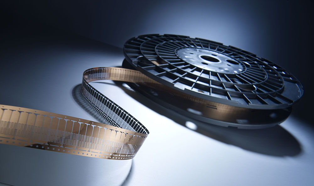
Stamping is an automated, high-speed process suitable for large production runs that make the requirement for initially high tooling costs tolerable. The sheet metal — typically in roll form — is pierced along both edges to create indexing holes that position the sheet during further processing. The location holes are used to advance the sheet metal strip through the stamping machine. Conventional stamping processes can provide an apparent cost advantage when precision, quality, and repeatability are less critical. However, these savings are quickly lost when secondary operations are needed to achieve flatness, functional edge precision, and exacting size features that are required for component performance in many applications. Stamping is usually utilised for the manufacture of an entire part or multiple whole parts which can be produced in one hit.

BENCHMARKING PCE
PCE is a metal processing technology that produces stress free, flat, components by selective etching through a photo-resist mask. It is especially well suited to the manufacture of precision parts such as grids and meshes, precision filters, sharp piercing or cutting edges, lead frames for integrated circuit boards, fuel cell and heat exchangers plates, precision springs, and washers and gaskets.
When compared with the above detailed conventional production processes, it has a number of inherent advantages, key among which are the ability to produce parts without degrading material properties, the fact that there is almost no limit on part complexity, and the ability to process a huge range of metals and alloys. Metals suitable for etching can be both ferrous and non-ferrous, and include austenitic and martensitic steels, coppers, brass and nickels. Hard to machine metals such titanium and its alloys, and aluminium can be processed, and also high temperature alloys such as Inconel, and precious metals including silver can also be machined.
When looking at each of the conventional processing technologies, each suffers from a number of drawbacks, key among which is the degradation of the material being processed due to high impact, or in the case of laser cutting the use of intense heat. However, the other key differentiator is in the area of tooling, which can be illustrated by comparing PCE to stamping. The tooling for PCE is digital or glass, so there is no need to start cutting expensive and difficult to adapt steel moulds. This means that large quantities of products can be reproduced with absolutely zero tool wear, ensuring that the first and millionth part produced are precisely the same.
Also, as the tooling is “virtual”, it can be adapted and changed extremely quickly and economically, making it ideally suited for anything from prototype runs to high volume production runs. This allows for design optimisation without financial penalty, and helps ensure a low risk entry strategy as well as facilitating easy product updating. Turnaround time using digital or glass tooling is about 90% less than that for stamped parts. Stamping requires substantial investment in mould fabrication which is not only costly but in some instances can take from six to ten months to complete, compared with a few hours for etching.
The economy and adaptability of the tooling for PCE is a key stimulus to design freedom, along with the ability to produce what may seem like impossibly complicated products. As the cost of creating prototypes is so low there is no barrier to entry with the technology, with complex designs being produced in a matter of days and designs iterations in a few hours. Perhaps the key drawback for industry in general is that in many instances, PCE is not part of some engineers’ repertoire, and because of this innovation can be somewhat stunted. PCE opens the door for innovation, and pushes back the barriers that constrain many design engineers and allows for the manufacture of parts many thought impossible.
COMPLEXITY
Many of today’s products are extremely complex and also very fragile. Indeed, in many instances, geometric complexity and the requirement for extremely exacting tolerances and precision mean that PCE is not just “a” potentially desirable manufacturing process, but is in fact the “only” technology able to make certain products.
Whether in low, medium, or high-volume applications, the complexity of a part adds cost when stamping. The complexity of a product requires complex tooling, and complex tooling means increased costs, increased chance of tool failure, and more time for satisfactory completion. For PCE it makes no difference how complex the geometry of the part is and therefore the complexity of the digital tooling. Costs and lead-times do not increase with this increased complexity.
PCE can produce finer detail than is possible with stamping, and there is no degradation and deformation of the metal being processed, and no burrs or defects produced. Failure rates are minimal, and every part produced is absolutely flat, which in some application is vital.
Stamping fabricates a product by pressing a substrate into a mould, and forming a shape. It is best suited economically to extremely high-volume runs where the tooling expense is justifiable, and where product geometry is not too complex.
PCE is a more complicated process, and so it can be applied to more complex geometries and can achieve exacting levels of precision. There are a number of variables in the process that can lead to tolerance creep, but such risks can be negated by utilizing the experience of a PCE specialist such as micrometal GmbH where advancements in PCE have been taken it far beyond the industry standard.
www.micrometal.de
About micrometal
micrometal GmbH (incorporating HP Etch and Etchform) specialises in the industrial production of highly precise metal components. The 3 companies photo-chemically etch very large numbers of parts for a multitude of industries with an accuracy that is unique. The companies etch a huge range of metals, and deliver customer-specific, clean, complex components, free of stress and burrs. micrometal’s, HP Etch’s and combined processes and expertise offer the right solution for every challenge. The companies provide a one-stop-shop to customers looking to benefit from a world-class photo-chemical etching service.
Micrometal Contact
t. +49 (0)7631 93688-0
e. info@micrometal.de
w. www.micrometal.de
Media Contact
t. +44 (0)7712 891070
e. chris@microprm.com
w. www.microprm.com